 |
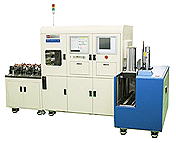
 Wafer Inspection& Sorting System Wafer Inspection& Sorting System |
High Productivity : Max 3,600 Wafers / Hour
Fully Available to Inspect & Measure the Wafer with High Performance
Vision Camera
Precise Saw Mark detection using Top & Bottom Laser Sensor
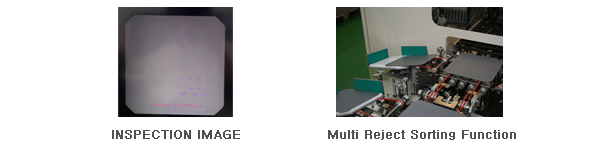
Detail Inspection Items
- 1st(Top)/2nd(BTM) Vision Station :
Geometry (Size, Surface, Stain, Saw Mark, etc)
- 3rd Vision Station : Micro crack
- 4th TTV & Resistivity measurement
- 5th Lifetime measurement
Multi Reject Wafer Sorting Function
Modular Type Structure
- Loader, Inspection Zone, Sorting Zone
Available to enlarge the Sorting Zone by Modular Docking Type Design
Solution for machine vibration
|
|