HANMI Semiconductor develops next-generation HBM process equipment…‘New Dual TC Bonder’ is about to be released
HANMI Semiconductor is going to release next-generation high-bandwidth memory (HBM) equipment. HBM is a high-performance memory used in artificial intelligence (AI), and is a semiconductor that has recently been increased in demand along with AI.
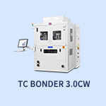
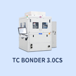
According to the industry on the 26th, HANMI Semiconductor is developing a new equipment called, ‘New Dual TC Bonder’. It is known that it will be released as early as the second half of the year at the latest stage of development.
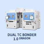
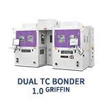
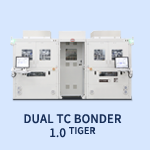
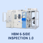
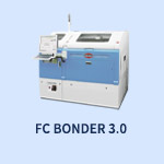
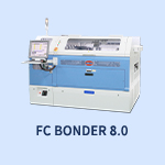
This equipment attaches and stacks semiconductor chips processed by the silicon penetration electrode (TSV) method to wafers. It serves to precisely stack individual chips by compressing them with heat.
TSV refers to electrodes that penetrate chips up and down by drilling thousands of fine holes in DRAM chips, which are essential for manufacturing high-performance 3D memory such as HBM.
Companies, which can implement this kind of process, are considered in one of the few due to the high technical difficulty of the entire process from drilling holes to stacking and attaching them.
HANMI Semiconductor is said to have applied the name ‘New Dual TC Bonder’ in the sense of second-generation equipment as it has succeeded in significantly improving productivity and precision compared to the first generation currently supplied to the market.
The development of next-generation equipment is drawing keen attention from the market because it is aimed at responding to the rapidly growing HBM market.
HBM is a high-performance memory that innovatively increases data processing speed compared to conventional DRAMs by connecting multiple DRAMs vertically.
For AI services such as Chat GPT, it is necessary to be able to process vast amounts of data smoothly, and high-performance and high-capacity semiconductors are essential.
HBM is a memory that has emerged in response to such market demands and is emerging as an AI necessity along with GPU.
According to market research firm ‘TrendForce’, HBM accounts for less than 1% of the total DRAM market, but it is expected to grow more than 45% annually from this year to 2025.
HBM is improving its performance by increasing its stacking to 2nd, 4th, 8th stages and more than that. The products released so far are the best in 8 layers, and the industry is about to mass-produce 12 layers.
HANMI Semiconductor is expected to accelerate its entry into the HBM market with next-generation equipment.
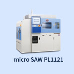
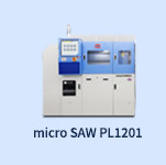
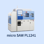
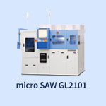
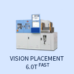
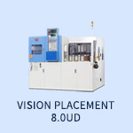
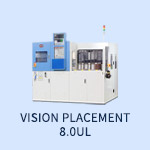
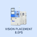
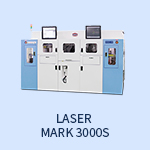
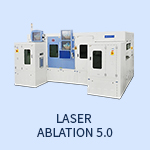
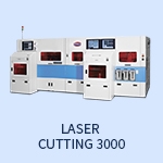
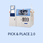
HANMI Semiconductor is a semiconductor post-process equipment company. It is making devices that cut, inspect, load, and stack semiconductor packages. In Korea, the proportion of overseas exports is unusually high.
In customer satisfaction survey organized by Techinsights, a semiconductor research company, it was the only Korean equipment company to be selected as one of the top 10 in customer satisfaction along with global semiconductor equipment companies such as ASML, Ram Research and Applied Materials.
A local corporation was established to target Vietnam, which has emerged as a new production base for global semiconductor manufacturers.